Infinite NOPs
The 6809E is running! Once the weekend began with the chip in my possession, like any good engineer I resisted the urge to immediately let out the blue smoke and instead sat down with the datasheet. The moment I saw the word “clock” I remembered that I hadn’t bought a 1MHz oscillator. Fortunately, rather than jumping in the car and driving to Halted, I continued reading and discovered that clocking wasn’t going to be easy.
The 6809E doesn’t take a single clock input like other processors I’ve seen (mostly AVRs and a few PICs). Instead, it has a Q input and an E input. Individually they look like regular 50%-duty square waves, but they’re synchronized, so you can’t just add two oscillators; rather, E’s rising edge must follow Q’s rising edge by at least 200ns (a fifth of a clock cycle on a 1MHz processor). If you draw this on paper, it ends up looking like E is simply phase-shifted by a quarter-cycle. I am not sure why Motorola made this an external requirement of the ‘09. The datasheet only says “this approach minimizes clock skew inherent with an internal buffer.” If I, as a system designer, am supposed to care about that, then I suppose there are external events that depend on the timing of the E edges. Still, it seems Motorola could have put the Q/E-generating circuitry in the chip, and run the E signal out on a pin.
Anyway, it’s a requirement. My first instinct was to get a trusty old ATtiny13A to generate the clock signals, but my first coding attempt produced only a 78kHz signal, below the 105kHz minimum frequency implied by the ‘09’s bus timing characteristics in the datasheet. I could have easily optimized the code; using back-of-the-envelope calculations, having 9.6 million AVR instructions per second and wanting maybe 500kHz cycles for now, that gave me about 19 instructions to generate a clock cycle, which ought to be easily doable. But I was ready for a break, and besides, it was time for lunch, so I decided to get out of the house.
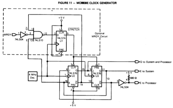
I returned with a 74HC109, which was the closest I could find on a Saturday to the 74LS76-based circuit in the datasheet:
I couldn’t find any oscillators at all, so I still had to use the ATtiny for the basic clock. After breadboarding it all up, I was getting a beautiful 300kHz Q/E signal out of the ‘109. Time to work the ‘09 into my circuit!
This part was tedious but straightforward. Wire up all the pins that can have a constant state for now (IRQ, HALT, etc.). Connect Q and E. Leave the address bus disconnected except for headers to attach logic-probe pins. Re-read the datasheet to make sure I wasn’t mixing up inputs and outputs. Count the pins to avoid expensive off-by-one errors.
The data pins are a neat trick that Quinn recently wrote about, and it helps to understand the reset process to appreciate it. On RESET’s rising edge, the processor reads a 16-bit address from the reset vector (at $FFFE), then jumps there and starts executing code. In a normal 6809-based computer, $FFFE would map to ROM, and the address in the vector would point to the reset routine, also in ROM. But we don’t have ROM yet, and even if we did, we don’t have any code to put in it. So instead, we choose a single byte and wire it manually to the D0-D7 pins. But which byte? In the case of the 6809, $12 is a good choice. It’s the NOP (no operation) opcode, which is always pretty safe to run. If we permanently set the data bus to $12, then this is the reset sequence:
- CPU reads the top half of the reset routine from $FFFE. It’s $12.
- CPU reads the bottom half of the reset routine from $FFFF. It’s $12, too. So the reset code starts at $1212. CPU jumps there.
- CPU reads the opcode at $1212. You guessed it: it’s $12. That’s a one-byte opcode, so it executes the operation, which does little more than increasing the program counter to $1213.
- CPU reads the opcode at $1213. It’s $12. And so on.
If our prediction is correct, on the address bus we should see this sequence: $FFFE, $FFFF, $1212, $1213, $1214, and so on. It’s not useful computation, but observing this sequence lets us know we’re running the CPU correctly.
Anyway, that’s the theory. In practice I saw the reset vector being read, then an orderly but mysterious sequence: 0, 1, F, 0, F, 0, 2, 3, F, 0, F, 0, 4, 5, F, 0, F, 0, 6, 7, F, 0, F, 0 (I love my Saleae Logic, but man I wish it had something like 64 inputs. Meanwhile, this is just the lower 4 bits of the address bus). Still, I was excited because I was seeing real signals coming out of the ‘09, which meant my clock circuit worked!
But I couldn’t figure out why the address bus wasn’t matching what I expected. I thought about changing the hardcoded data bus to $0E, which would have put it into a perma-loop JMPing from $0E0E to $0E0E. I began moving the data jumpers, and _noticed that their bus strip wasn’t connected to anything!_ The data bus had been floating, and the ‘09 (bless its heart) responded by reading the pins as zeroes. The weird sequence earlier now made sense, as NEG is opcode $00, takes a single-byte argument, and completes in six cycles. The CPU was already exceeding my expectations: I’d asked it to do nothing but cycle through instructions, and it was busily negating address $0! (_I’m still not convinced this is correct. Why would NEG take a single-byte argument, rather than a two-byte address? Is this an odd 6809 architecture limitation?) _Update: the 6809 has this cool mode called “Direct,” which takes the high 8 bits from a register, and the low 8 bits from the opcode argument. This is why 0, 0 translated to NEG $0000. It’s a little like x86 segment registers, but without the intense pain!
Hooking the bus up properly to Vcc and GND gave the expected results, jumping to $1212 and quickly working its way up the address space. Excellent!
After a break for dinner, I decided to switch over to software for a while. I got the ATtiny’s pure bit-banging Q/E generation code up to about 300kHz, so I was able to ditch the ‘109 for now. (That code is now checked in.) Although I think it’s cool to have hacked the clock signal without an oscillator, I’m pretty sure I’ll relent and get a real 4MHz oscillator, because I want Joust to run at the correct, original speed, and it would be a lot of avoidable work to get the ATtiny oscillating at exactly the right rate.